LM358P Op Amp: Description, Features, Package, Usage, Equivalents
2024-04-17
4622
The LM358P is a Low Power, Dual Op Amp Amplifier. It can operate in a wide range of single-supply applications with a high gain-bandwidth product and integrated noise. This article will introduce it in detail from the aspects of features, package, layout, and application.
Catalog
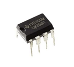
Figure 1: LM358P
LM358P Description
The LM358P is the next-generation version of the industry-standard operational amplifier LM358 and contains two high-voltage (36V) operational amplifiers. These devices provide excellent value for cost-sensitive applications and feature low offset (300µV typical), common-mode input range to ground, and high differential input voltage capabilities. In addition, LM358P is packaged in DIP for easy manual soldering.
The LM358P consists of two independent high-gain frequency-compensated operational amplifiers designed to operate from a single power supply over a wide voltage range. This circuit can realize single power supply operation within the power supply voltage range of 3V to 32V, and also supports independent operation under dual power supply conditions, and has an internal frequency compensation function. The LM358P op amp simplifies circuit design and features enhancements such as unity-gain stability, lower offset voltage (3mV maximum), and lower quiescent current per amplifier (300µA typical), making it suitable for environmentally challenging applications.
Alternatives and Equivalents
Characteristics of LM358P
Wide supply range of 3 V to 36 V
Internal RF and EMI filter
Quiescent current: 300 µA/ch
2-mV input offset voltage max. at 25°C
3-mV input offset voltage max. at 25°C
Unity-gain bandwidth of 1.2 MHz
Common-mode input voltage range includes ground, enabling direct sensing near ground
On products compliant to MIL-PRF-38535, all parameters are tested unless otherwise noted. All other products, production processing does not necessarily include testing of all parameters.
Package Design of LM358P
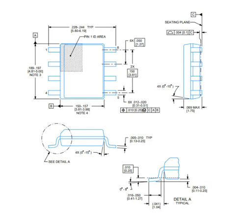
Figure 2: Package Design of LM358P
Layout of LM358P
Layout Guidelines
For the best operational performance of the device, use good PCB layout practices, including:
Noise can propagate into analog circuitry through the power pins of the circuit as a whole, as well as the operational amplifier. Bypass capacitors are used to reduce the coupled noise by providing low-impedance power sources local to the analog circuitry. Connect low-ESR, 0.1-µF ceramic bypass capacitors between each supply pin and ground, placed as close to the device as possible. A single bypass capacitor from V+ to ground is applicable for single supply applications.
Isolating the ground connections for analog and digital components within circuitry stands as a straightforward yet highly efficient approach to mitigate noise. Typically, one or more layers within multilayer PCBs are designated for ground planes, aiding in heat dissipation and minimizing EMI interference. Make sure to physically separate digital and analog grounds, paying attention to the flow of the ground current.
To reduce parasitic coupling, run the input traces as far away from the supply or output traces as possible. If it is not possible to keep them separate, it is much better to cross the sensitive trace perpendicular as opposed to in parallel with the noisy trace.
Place the external components as close to the device as possible. Keeping RF and RG close to the inverting input minimizes parasitic capacitance, as shown in the following figure.
Keep the length of input traces as short as possible. Always remember that the input traces are the most sensitive part of the circuit.
Consider a driven, low-impedance guard ring around the critical traces. A guard ring can significantly reduce leakage currents from nearby traces that are at different potentials.
Layout Examples
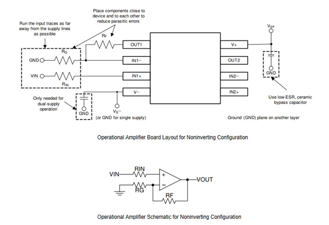
Figure 3: Layout Examples
LM358P Uses
Some of the major applications of LM358P IC are listed below:
POS (point-of-sale) systems
Refrigerators, washers, and dryers
Air conditioners, both indoors and out
Voltage frequency drives, string inverters, central inverters, and AC inverters
Loop control and regulation
Motherboard and desktop PC
Power supplies that are uninterruptible
Integrator, adder, differentiator, voltage follower etc.
AC induction, brushed DC, brushless DC, high-voltage, low-voltage, permanent magnet, and stepper motors are all examples of motor control
LM358P Circuit
Light Sensor Circuit
The circuit shown above is a light sensor circuit built around an LM358 IC. In this configuration, the IC is used as a comparator. The LED is connected to the output, i.e., pin 1, and is associated with operational amplifier part 1 or A. The sensitivity of the circuit can be adjusted with a 20K variable resistor.
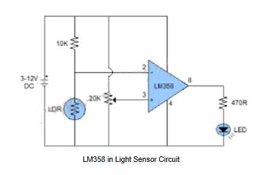
Figure 4: LM358 in Light Sensor Circuit
Dark Sensor Circuit
The circuit shown above is a dark sensor circuit with LM358 IC as the core. In this circuit, the center pin of the variable resistor is connected to pin 2, which corresponds to the inverting input of the A part of the IC. Thus, when in complete darkness or low light, the circuit produces a high output from part A. The exact result depends on the adjustment of the 20K variable resistor.
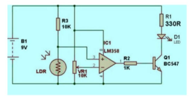
Figure 5: LM358 in Dark Sensor Circuit
Can LM358 and LM358P Be Replaced?
LM358 and LM358P are the same model of operational amplifier chips, and their main difference lies in the package form. LM358P uses DIP (dual in-line package), which is more convenient for manual installation; while LM358 uses SOIC (small outline integrated circuit package), which is more suitable for automated production. Although the package forms are different, the parameters and specifications of the two are basically the same, such as input bias current, input bias voltage, and gain bandwidth product.
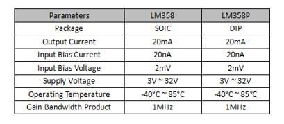
Figure 6: LM358 Vs. LM358P
It should be noted that there may be slight differences between LM358 and LM358P produced by different manufacturers. Therefore, in practical applications, we should choose the appropriate model and manufacturer according to specific needs. Generally speaking, LM358 and LM358P are different package forms of the same operational amplifier. They have the same electrical parameters and functions, so they can be used interchangeably. Among them, LM358P adopts a more anti-static package, which is more suitable for use in harsh environments. However, in most cases, the two models are interchangeable. In order to ensure the stability and performance of the circuit, it is recommended to carefully consult the relevant data sheet before use to confirm whether its parameters and package are suitable for the specific application.
How to Use LM358P Correctly in Circuit Design?
When using LM358P, we need to consider the following aspects.
Input and Output Matching
We need to make sure that the levels of the input and output signals match the input and output ranges of the LM358P. If the input signal is out of the LM358P's operating range, it may cause distortion or damage to the device.
Pin Connections
When connecting the LM358P, we first need to clarify the function of each pin before we can ensure that they are properly wired into the circuit. For example, the input pins need to be connected to a signal source in order to receive the input signal, while the output pins need to be connected to a load in order to output the processed signal. The power pins need to be connected to a stable power source, while the ground pins need to be grounded to ensure proper power supply to the circuit. At the same time, we also need to pay attention to the connection order and polarity of the pins, so as not to cause circuit failure due to connection errors.
Thermal Design
Poor heat dissipation may cause the performance of the LM358P to deteriorate, or even lead to overheating damage. Therefore, we need to fully consider the heat dissipation problem when designing the circuit. A common method of heat dissipation is to increase the heat sink around the operational amplifier to increase the heat dissipation area and improve the efficiency of heat dissipation.
Frequency Compensation
For some applications, frequency compensation may be required to ensure the stability of the LM358P. In practice, we first need to determine the amount of compensation required according to the application requirements, and then select the appropriate capacitance value. Next, we connect the positive terminal of the capacitor to the compensation pin of the LM358P and ground the negative terminal of the capacitor. In this way, the capacitor can form an RC network with the resistor inside the amplifier, thus realizing frequency compensation.
Protection
In order to ensure the stable operation of the LM358P operational amplifier and to prolong its service life, we should consider adopting a protection circuit to guard against the effects of over-voltage, over-current, and other undesirable conditions. Specifically, we can achieve effective protection against overvoltage by adding a series resistor to the input or using a specialized overvoltage protection device. Meanwhile, in order to control the current, we can use devices such as current limiters or fuses to ensure that the current flows within a safe range.
Power Supply
Please make sure to provide the proper supply voltage for the LM358P. The LM358P can usually operate in both single-supply mode and dual-supply mode, depending on our application requirements. If we choose to use a single power supply, then please make sure that the supply voltage is not lower than the minimum operating voltage required by the LM358P. If we choose to use a dual power supply, then we need to provide both positive and negative supply voltages.
Maintain Good Layout and Grounding
When designing the board, we need to make sure that there is a good connection between the signal and power ground to minimize noise and interference. When laying out the board, we should keep the signal ground close to the power ground and try to avoid signal lines crossing the power ground. In addition, using a low impedance ground path reduces the resistance and inductance of the ground wire, which further reduces noise. Meanwhile, in order to ensure the stability of the power supply and reduce power supply noise, we need to use thicker or wider wires to connect the power supply ground to reduce the resistance and inductance of the power supply line.
Frequently Asked Questions [FAQ]
1. What is the function of LM358P?
The LM358 has several applications, including operational amplifier (Op-amp) circuits, transducer amplifiers, DC gain blocks, comparator circuits, Active filters, current loop transmitters for 4 to 20mA and so on.
2. What is the difference between LM358P and LM358N?
According to the National Semiconductor Corporation's standard P and N is the device package form. The package of LM368N is a plastic dual in-line package. LM358P should be a single in-line package.
3. What is the difference between LM358P and 741?
Difference between LM358 & LM741 is, LM358 is newer and has two OP-AMP on chip while in 741 only one OP-AMP is present. Both the IC's have 8 pins.
4. What is LM358P description?
It has two independent op-amps with a single power supply in one IC package. This IC can also operate from the split power supply and the magnitude of the power supply does not affect the low power supply current drain.
 ABOUT US
Customer satisfaction every time. Mutual trust and common interests.
function test. The highest cost-effective products and the best service is our eternal commitment.
Hot Article
- Are CR2032 and CR2016 Interchangeable
- MOSFET: Definition, Working Principle and Selection
- Relay Installation and Testing, Interpretation of Relay Wiring Diagrams
- CR2016 vs. CR2032 What’s the difference
- NPN vs. PNP: What's the Difference?
- esp32 vs stm32: which microcontroller is better for you?
- LM358 Dual Operational Amplifier Comprehensive Guide: Pinouts, Circuit Diagrams, Equivalents, Useful Examples
- CR2032 VS DL2032 VS CR2025 Comparison Guide
- Understanding the Differences ESP32 and ESP32-S3 Technical and Performance Analysis
- Detailed Analysis of RC Series Circuit
 TL431 Voltage Regulator Detailed Guide
2024-04-17
 74LS138 Decoder Working Principle, Application Scenarios and 7AHC138 vs 74LS138
2024-04-16
Hot Part Number
 GRM033R61E103KA12D
 CGA3E3X7R1H224M080AB
 UMK105CG020BV-F
 12061E104MAT2A
 06033A301GAT2A
 1206AC101JAT1A
 BSC040N10NS5ATMA1
 LC4064ZC-75MN56C
 PIC16F73T-I/SO
 CY62137FV30LL-45ZSXIT
- V375A24C600BL
- VI-274-CX
- EPM240GM100I5N
- A3P060-CSG121
- MK30DX128VMC7
- M30281FAHP#U5B
- VE-2W1-EW
- ERA-6AEB1691V
- VI-JWZ-CY
- FP75R12KT4-B16
- NCV33204DR2G
- XC9536XL-10VQ64I
- T491B475K016AT7280
- LM3478MM
- UC3875DWPTR
- T491B106M016AT7010
- TPS62153RGTR
- BQ20Z45DBTRG4
- CY283310C
- KFG1216Q2A-DEB5
- LT1019CS8-4.5
- PCI4410PDV
- PCK2002PLPWDH
- PCT25VF032B-80-4I-S2AF
- TC74HC238A
- TS3A23157DGSR
- UPD78P218AGC
- 74LVC244D
- FL129PIFS
- GMS97C54
- GMS97L52Q
- N13P-GV-S-A2
- RTL8671BH
- UPD6345GS-E1
- N80L188EB13
- K4ZAF325BM-HC14
- STM32L452RCT6TR
- SC14CVM1.9FLN
- MTFC4GLDDQ-4M