Exploring IC 7400: Specifications, Pin Configuration, and Practical Applications
2024-09-09
4460
Catalog
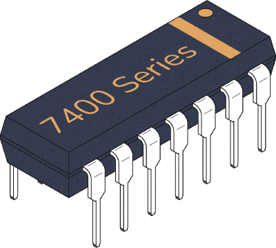
Figure 1: IC 7400
What Is IC 7400?
The IC 7400 is a versatile digital logic component used in a wide range of electronic systems. Its adaptability makes it useful to devices ranging from basic logic circuits to more complex components like Arithmetic Logic Units (ALUs) and bus transceivers. As part of the 7400 series, this IC is designed to serve as a building block for digital operations. It supports functions like basic logic gates (AND, OR, NAND, NOR), data storage with registers, Random Access Memory (RAM) modules, and even decoding units for tasks such as converting binary to decimal. The IC 7400 is particularly valued for its four independent 2-input NAND gates, which are used in both combinational and sequential logic designs. Each gate has two input pins and one output pin, while the remaining two pins provide power (Vcc) and ground (GND). These connections are ideal for stable performance and reliable operation.
IC 7400 Pin Configuration
Understanding the IC 7400's pin configuration is perfect for achieving desired circuit behavior. Each pin has a specific role that influences the IC’s overall function in the system.
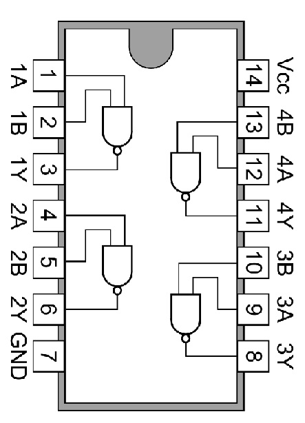
Figure 2: IC 7400 Pin Configuration
• Pin 1 (A-input for the first gate) – One of two inputs for the first NAND gate. The signal connected here must work with Pin 2 to determine the output logic state at Pin 3.
• Pin 2 (B-input for the first gate) – The second input for the first NAND gate. It pairs with Pin 1, and when both inputs are high, the output (Pin 3) will be low, as per NAND gate logic.
• Pin 3 (Y-output for the first gate) – The output of the first NAND gate, providing the inverted result of the AND operation between Pins 1 and 2. Engineers monitor this output during testing, often using oscilloscopes or logic analyzers to verify proper signal behavior.
• Pin 4 (A-input for the second gate) – Similar to Pin 1 but for the second NAND gate, this pin receives input in more complex designs.
• Pin 5 (B-input for the second gate) – Pairs with Pin 4 to control the output at Pin 6.
• Pin 6 (Y-output for the second gate) – The second NAND gate’s output, used in forming more complex logic circuits or controlling later stages in the design.
• Pin 7 (Ground) – This pin connects to the ground of the circuit, serving as the IC’s reference point. Incorrect grounding can result in erratic behavior or complete failure of the IC.
• Pin 8 (Y-output for the third gate) – Output for the third NAND gate, monitored during debugging to ensure correct operation.
• Pin 9 (B-input for the third gate) – Input for the third gate, paired with Pin 10.
• Pin 10 (A-input for the third gate) – Works with Pin 9 to generate the output at Pin 8.
• Pin 11 (Y-output for the fourth gate) – The final gate’s output, used for driving final-stage logic operations.
• Pin 12 (B-input for the fourth gate) – Input for the last NAND gate, paired with Pin 13.
• Pin 13 (A-input for the fourth gate) – Input that, together with Pin 12, determines the state of the output at Pin 11.
• Pin 14 (Positive supply voltage) – Supplies the IC’s power. Engineers ensure this 5V input remains stable by using decoupling capacitors to filter out noise and maintain consistent voltage delivery.
Specifications
The IC 7400 has specifications that make it a reliable choice for many digital circuit designs, balancing power, speed, and compatibility with multiple logic families.
• Operating voltage: 5V
Engineers use voltage regulators to keep this input steady, preventing logic faults caused by voltage fluctuations.
• Propagation delay: 10 ns
The time it takes for a signal to travel from input to output. While sufficient for most applications, engineers account for this delay in high-speed circuits, using oscilloscopes to confirm that all timing is within acceptable bounds.
• Maximum toggle frequency: 25 MHz
This sets the speed limit for how quickly gates can switch between states. Engineers must ensure their design operates below this frequency to avoid errors in fast-switching circuits.
• Power consumption per gate: Up to 10 mW
Low power consumption allows multiple ICs to be used without overloading the power supply. In large systems, engineers perform careful power budgeting to ensure efficiency.
• Composition: Four independent 2-input NAND gates
The modular design of the IC allows engineers to build complex logic systems with just a few basic components.
• Output compatibility: TTL, NMOS, CMOS
Compatibility with various logic families ensures smooth integration into mixed-technology systems. Engineers often use resistors to balance mismatched voltages between logic families.
• Operating voltage range
While the IC typically runs at 5V, it can handle different voltages, allowing it to adapt to various system environments.
• Versatile operating conditions
The IC operates reliably across different environments. In extreme temperatures, engineers implement heat sinks or cooling systems to maintain performance.
7400 Family ICs
The 7400 series includes a range of digital logic ICs, each serving specific roles in circuit design. Below are common ICs and their practical applications:
IC 7400 (Quad 2-input NAND gate)
Used for basic logic functions, signal inversion, and sequential logic operations, the 7400 is a staple in both simple and complex designs.
IC 7402 (Quad 2-input NOR gate)
Engineers use this for circuits requiring default low output unless inputs are activated. It’s ideal for power-sensitive designs.
IC 7404 (Hex inverter)
Inverts logic levels, perfect for synchronization and timing adjustment.
IC 7400 NAND Gate Circuit Design

Figure 3: IC 7400 Circuit Design with NAND Logic
The IC 7400's four independent 2-input NAND gates offer flexibility, allowing any basic logic gate to be constructed. This makes the IC a go-to tool for educational and professional circuit designs. Engineers often use it to construct complex circuits, such as flip-flops or multiplexers, simplifying design and testing phases.
During assembly, engineers ensure proper signal integrity to avoid errors. Oscilloscopes or logic analyzers help verify the accuracy of signal transitions, particularly in high-speed applications. In temperature-sensitive environments, engineers use thermal management to ensure the IC operates reliably without signal degradation.
Advantages and Disadvantages
|
Advantages |
Disadvantages |
|
Cost-effective:
Affordable for both professionals and hobbyists |
Power
consumption: Higher than newer CMOS options |
|
Versatile:
Useful for both simple and complex digital operations |
Speed
limitations: Maxes out at 25 MHz |
|
Easy
to use: Intuitive pin layout simplifies prototyping |
Limited
gates: Only four per IC, requiring more components for complex designs |
|
Widely
available: Easy to source from multiple suppliers |
Outdated
technology: Less suitable for cutting-edge applications |
|
Reliable:
Resists electrical noise and maintains stable performance |
|
Applications
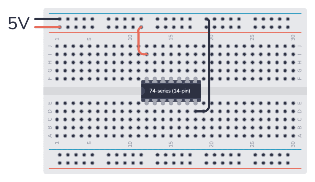
Figure 4: IC 7400 in Digital Electronics Application
The IC 7400 is widely used in various systems:
Security Systems: Processes inputs from motion or door sensors to trigger alarms.
Alert Systems: Monitors freezer temperatures and triggers alerts if thresholds are crossed.
Theft Alarms: Detects changes in light levels and triggers alarms, often in light-sensitive theft systems.
Automation: Controls water distribution in automated irrigation systems by processing soil moisture levels.
In all these applications, the IC 7400 ensures reliable decision-making with simple, powerful logic configurations. Its adaptability and ease of integration make it a preferred choice across multiple industries.
Conclusion
The IC 7400 continues to be a trusted component in digital circuit design due to its robust functionality, flexibility, and cost-effectiveness. While newer technologies may offer faster speeds and lower power consumption, the IC 7400 remains a valuable option for engineers and hobbyists alike. Its ability to handle diverse tasks—from security systems to automated irrigation—demonstrates its versatility. The IC 7400’s proven reliability and ease of integration make it a cornerstone in both legacy systems and contemporary digital logic designs, ensuring its ongoing utility across various industries and applications.
function test. The highest cost-effective products and the best service is our eternal commitment.
Hot Article
- Are CR2032 and CR2016 Interchangeable
- MOSFET: Definition, Working Principle and Selection
- Relay Installation and Testing, Interpretation of Relay Wiring Diagrams
- CR2016 vs. CR2032 What’s the difference
- NPN vs. PNP: What's the Difference?
- esp32 vs stm32: which microcontroller is better for you?
- LM358 Dual Operational Amplifier Comprehensive Guide: Pinouts, Circuit Diagrams, Equivalents, Useful Examples
- CR2032 VS DL2032 VS CR2025 Comparison Guide
- Understanding the Differences ESP32 and ESP32-S3 Technical and Performance Analysis
- Detailed Analysis of RC Series Circuit
 SPICE: Primary Dynamics, Applications, and Advantages
2024-09-10
 What Is Ball Grid Array (BGA)? Benefits, Types, Assembly Process
2024-09-09
Frequently Asked Questions [FAQ]
1. What is the difference between IC 7400 and IC 7402?
The difference between the IC 7400 and IC 7402 lies in the type of logic gates they contain: the IC 7400 has four independent 2-input NAND gates, while the IC 7402 has four independent 2-input NOR gates. In practical terms, the NAND gate outputs low only when both inputs are high, whereas the NOR gate outputs high only when both inputs are low. This means the IC 7400 is often used for universal logic circuits, while the IC 7402 is better suited for applications needing low output unless triggered by active inputs.
2. What is the difference between IC 7400 and IC 7408?
The IC 7400 and IC 7408 differ in the logic functions they provide. The IC 7400 contains four independent 2-input NAND gates, which output low only when both inputs are high. In contrast, the IC 7408 contains four independent 2-input AND gates, which output high only when both inputs are high. Practically, engineers use the IC 7400 for circuits requiring logic inversion and universal gate configurations, while the IC 7408 is used where straightforward conditional "AND" operations are required.
3. How do you connect a 7400 NAND gate?
To connect a 7400 NAND gate, you begin by connecting the Vcc pin (Pin 14) to the positive voltage supply and the GND pin (Pin 7) to ground. For each NAND gate, connect the two input pins (e.g., Pin 1 and Pin 2 for the first gate) to the input signals. The output (Pin 3 for the first gate) will reflect the NAND logic, where the output is low only when both inputs are high. Ensure correct wiring of input signals and power to avoid misfires in the logic operation.
4. What are the limitations of using IC 7400 in modern electronics?
The limitations of using the IC 7400 in modern electronics stem from its higher power consumption compared to newer CMOS alternatives, slower operational speed (max 25 MHz), and limited functionality with only four NAND gates per chip. In high-performance, power-sensitive, or miniaturized applications, engineers often choose more advanced logic ICs with faster speeds, lower power consumption, and higher integration to meet current technology standards.
5. How can I test IC 7400 functionality?
To test the functionality of the IC 7400, first power it by connecting Pin 14 to Vcc (5V) and Pin 7 to GND. Apply known logic inputs to the NAND gate's input pins (e.g., Pins 1 and 2) and measure the output at the corresponding output pin (e.g., Pin 3). Use a multimeter or oscilloscope to verify that the output matches the expected NAND gate logic, where the output should only be low when both inputs are high. Repeat the process for each gate to ensure all gates are functioning properly.
Hot Part Number
 CL21F104ZBCNNNC
 2225PC105MAT1A
 CC0805JRX7R9BB272
 12065A200JAT4A
- 12063A511FAT2A
 CGA8N4X7R2J104M230KE
 GRM1555C1H5R7WZ01D
 TAJP685M010RNJ
 TAJT686K004RNJ
 TAP475M025F
- S9S08DZ60F2MLF
- ICL3232CB-T
- NCP21WF104J03RA
- VE-231-EX
- RSO-4805SZ
- AD8667ARZ-REEL7
- LMR23610AQDDARQ1
- SN65LVDS32D
- T491B226M016AT40537111
- UCC38C40DGKR
- AD8348ARUZ-REEL7
- ADUM3190SRQZ-RL7
- M74HC160RM13TR
- LTC2656CIUFD-L16#PBF
- AD7503KN
- AD5270BRMZ-50-RL7
- R5F101MJDFB#30
- ADV7280BCPZ-M
- TLV431BQDBZTG4
- AD8429BRZ
- DS1306EN+T
- LP3912RLX
- MT48LC2M8A1TG-10S
- N25Q128A13EF840F
- NT5CC64M16FP-DI
- R5F212D8SDFP
- TB62705CF
- TJA1051T/3/CM
- TMS320TCI6484CMH
- UPD72001GC-11
- FA5531N-A2-T1
- AD8018ARU
- S1X58174B00B0
- SAA2003H
- MT29C4G48MAPLCJA-5IT
- XC4010-5PC84C
- HT7A6312
- RV30YN20SB102
- MT48LC8M16A2P-6A:LTR