74HC02 Quad 2-Input NOR Gate Guide
2024-11-16
704
Catalog
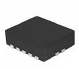
74HC02 Pin Configuration
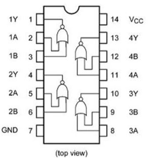
CAD Design for 74HC02

74HC02 Comprehensive Analysis
The 74HC02 is a quad 2-input NOR gate IC with built-in clamp diodes on its inputs, allowing it to interface with voltages above VCC when used with current-limiting resistors. It operates over a 2V to 6V supply range, making it compatible with both TTL and CMOS logic levels. The 74HC02 is ideal for digital logic applications that require reliable NOR gate operations, flexible voltage interfacing, and efficient performance in low-power circuits.
Characteristics of 74HC02
Wide Range of Supply Voltage
The 74HC02 operates seamlessly with supply voltages ranging from 2.0V to 6.0V. This broad compatibility allows integration with a diverse set of circuit designs, accommodating devices that function on low-power batteries as well as intricate electronic systems. We find this flexibility useful when crafting products for varied environments.
Efficient Power Use
Being a CMOS device, the 74HC02 features reduced power consumption, enhancing the operational lifespan of battery-based devices and lowering energy expenditures in larger setups. In mobile and embedded applications, the drive toward power-efficient components is increasingly evident, aligning with broader ecological goals to minimize environmental impact.
Superior Noise Immunity
The 74HC02's capacity to ward off unwanted electrical interference ensures consistent operation even amidst high electromagnetic disturbances. This quality is to uphold signal integrity, especially in industrial environments or densely packed circuit boards where interference is an ongoing challenge.
Strong Latch-Up Defense
Demonstrating a latch-up current capability surpassing 100 mA based on JESD 78 standards, the 74HC02 showcases exceptional durability. Its ability to resist latch-up is instrumental in defending circuits from potential failures, thereby strengthening overall system reliability. This feature proves advantageous in contexts by reducing maintenance requirements and extending the lifespan of the devices.
Adherence to Logic Level Standards
Operating at the CMOS level, the 74HC02 contrasts with the TTL-aligned 74HCT02, both conforming to JEDEC standards. This distinction allows for adaptability to various logic standards, thereby easing integration into diverse digital circuit architectures. We find it straightforward to align these components with pre-existing hardware, resulting in improved compatibility and fewer design limitations.
Protection Against Electrostatic Discharge (ESD)
Equipped with ESD safeguards adhering to HBM and MM standards, the 74HC02 is well-shielded against static discharge incidents. This protection handling and installation, stages where static electricity could pose serious risks. By adhering to best practices in ESD management, we can decrease the likelihood of component damage and failure.
Flexible Packaging and Temperature Tolerance
With a variety of packaging options, the 74HC02 meets diverse application demands, showing adaptability in both space-limited and high-temperature settings. Its operational temperature span from -40°C to +125°C ensures reliability in extreme conditions, ranging from frigid outdoor settings to sweltering industrial environments. This adaptability is often for applications where maintaining consistent performance despite temperature variations is deemed requiredl.
Technical Specifications
The 74HC02 ideally operates within a supply voltage range spanning from 2V to 6V, fostering adaptability across numerous digital systems. With ease, it melds into current circuits due to this wide range. Similarly, the Nexperia USA Inc. 74HC02BQ,115 offers an equivalent voltage spectrum, emphasizing its broad applicability in varying technological contexts. Here are the specifications, attributes, parameters of the Nexperia USA Inc. 74HC02BQ,115.
|
Type |
Parameter |
|
Factory Lead Time |
8 Weeks |
|
Contact Plating |
Gold |
|
Mount |
Surface Mount |
|
Mounting Type |
Surface Mount |
|
Package / Case |
14-VFQFN Exposed Pad |
|
Number of Pins |
14 |
|
Logic Level-High |
1.5V ~ 4.2V |
|
Logic Level-Low |
0.5V ~ 1.8V |
|
Operating Temperature |
-40°C~125°C |
|
Packaging |
Tape & Reel (TR) |
|
Series |
74HC |
|
Published |
2013 |
|
JESD-609 Code |
e4 |
|
Part Status |
Active |
|
Moisture Sensitivity Level (MSL) |
1 (Unlimited) |
|
Number of Terminations |
14 |
|
Max Power Dissipation |
500mW |
|
Voltage - Supply |
2V~6V |
|
Terminal Position |
DUAL |
|
Number of Functions |
4 |
|
Supply Voltage |
5V |
|
Terminal Pitch |
0.5mm |
|
Base Part Number |
74HC02 |
|
Pin Count |
14 |
|
Number of Outputs |
1 |
|
Output Voltage |
6V |
|
Operating Supply Voltage |
5V |
|
Supply Voltage-Max (Vsup) |
6V |
|
Supply Voltage-Min (Vsup) |
2V |
|
Power Dissipation |
500mW |
|
Output Current |
25mA |
|
Propagation Delay |
15 ns |
|
Quiescent Current |
2μA |
|
Turn On Delay Time |
7 ns |
|
Family |
HC/UH |
|
Logic Function |
NOR |
|
Number of Inputs |
2 |
|
Logic Type |
NOR Gate |
|
Number of Gates |
4 |
|
Max Propagation Delay @ V, Max CL |
15ns @ 6V, 50pF |
|
Number of Input Lines |
8 |
|
Length |
3mm |
|
Radiation Hardening |
No |
|
RoHS Status |
ROHS3 Compliant |
|
Lead Free |
Lead Free |
Comparable Components
|
Parameter |
74HC02BQ,115 |
SN74HC02DBR
|
74HC02BQ-Q100,115
|
SN74HC02DE4
|
SN74HC02NSR
|
|
Manufacturer |
Nexperia USA Inc. |
Texas Instruments |
Nexperia USA Inc. |
Texas Instruments |
Texas Instruments |
|
Package / Case |
14-VFQFN Exposed Pad |
14-SOIC (0.209, 5.30mm) |
14-SSOP (0.209, 5.30mm) |
14-VFQFN Exposed Pad |
SOIC |
|
Number of Inputs |
2 |
2 |
2 |
2 |
- |
|
Number of Pins |
14 |
14 |
14 |
14 |
14 |
|
Logic Function |
NOR |
NOR |
NOR |
NOR |
NOR |
|
Propagation Delay |
15 ns |
15 ns |
15 ns |
15 ns |
15 ns |
|
Supply Voltage |
5 V |
5 V |
5 V |
5 V |
5 V |
|
Quiescent Current |
2 μA |
2 μA |
2 μA |
2 μA |
2 μA |
|
Technology |
CMOS |
CMOS |
CMOS |
CMOS |
CMOS |
74HC02 Functional Schematic
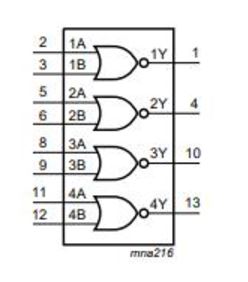
Circuit Diagram for 74HC02
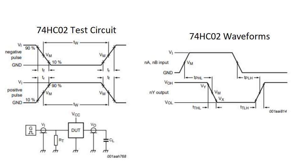
Datasheet PDF
74HC02BQ,115 Datasheets
74HC02BQ,115.pdf74HC02BQ,115 Details PDF
74HC02BQ,115 PDF - DE.pdf
SN74HC02DBR Datasheets
SN74HC02DBR.pdfSN74HC02DBR Details PDF
SN74HC02DBR PDF - DE.pdf
SN74HC02DE4 Datasheets
SN74HC02DE4.pdfSN74HC02DE4 Details PDF
SN74HC02DE4 PDF - DE.pdf
SN74HC02NSR Datasheets
SN74HC02NSR.pdfSN74HC02NSR Details PDF
SN74HC02NSR PDF - DE.pdf
 ABOUT US
Customer satisfaction every time. Mutual trust and common interests.
function test. The highest cost-effective products and the best service is our eternal commitment.
Hot Article
- Are CR2032 and CR2016 Interchangeable
- MOSFET: Definition, Working Principle and Selection
- Relay Installation and Testing, Interpretation of Relay Wiring Diagrams
- CR2016 vs. CR2032 What’s the difference
- NPN vs. PNP: What's the Difference?
- esp32 vs stm32: which microcontroller is better for you?
- LM358 Dual Operational Amplifier Comprehensive Guide: Pinouts, Circuit Diagrams, Equivalents, Useful Examples
- CR2032 VS DL2032 VS CR2025 Comparison Guide
- Understanding the Differences ESP32 and ESP32-S3 Technical and Performance Analysis
- Detailed Analysis of RC Series Circuit
 LM321 Operational Amp: Pin Configuration, Applications, and Alternatives
2024-11-18
 Your Guide to IRLZ44N Power MOSFET
2024-11-16
Frequently Asked Questions [FAQ]
1. What Role does the 74HC02 Gate Serve?
The 74HC02 consists of a quad 2-input NOR gate, designed for interfacing with voltages beyond VCC through the use of clamp diodes. This setup not only increases its flexibility but also highlights the adaptability of these gates in various electronic designs. The NOR gate plays a role in digital logic circuits, as evidenced by its widespread presence in numerous digital systems.
2. Who Holds the Rights to the 74HC02 Datasheet?
Fairchild Semiconductor owns the copyright to the datasheet, which serves informational purposes. The broad distribution of such documentation and comprehension in both educational and professional technology sectors.
3. When Was the SN54HC02 SCLS076G First Introduced?
The SN54HC02 SCLS076G was initially released in December 1982 and underwent revisions until December 2020. These updates exhibit the continuous evolution regarding its availability, warranty, and applications, keeping it pertinent and effective in changing technological environments.
4. What Defines a NAND Logic Gate?
A NAND gate exclusively provides a false output when all inputs are true; otherwise, it outputs a high signal if any input is low. This contrasts with an AND gate, illustrating a complexity that supports the core framework of many logic circuits by offering alternative routes for signal processing.
Originating from Sheffer's 1913 findings, the NAND operation forms a cornerstone of logic operations within modern integrated circuits and computers. It holds significance not only in models but also in this implementations that guide the integrity and logic of computational systems.
5. What is the Voltage Range for Operating a 74HC02 OR Gate Chip?
The 74HC series functions within a flexible voltage range of 2 to 6 volts, with input and output levels dependent on specific operating conditions. This versatility is mirrored across numerous applications, the role of these specifications in adapting to various operational contexts and boosting component efficiency.
Hot Part Number
 C0603C0G1H820J030BA
 08051A3R9CAT2A
 CC0402KRX7R9BB223
 CL10B224MO8NNNC
 GCM31A7U2J150JX01D
 06035A240JAT2A
 CC0603JRNPOABN101
 1812HC102ZAT1A
 1808AA102MAT1A
 06035C472KAJ2A
- AK5394AVS
- AFS600-FG484I
- MCZ33884EGR2
- AS4C128M8D2-25BCN
- MT41K256M8DA-107:K
- ISL28022FUZ-T7A
- 6N135S-TA1
- MAX3313ECUB+T
- RT0402BRE0716KL
- FD800R17KF6C_B2
- PM150RFE060
- AD8428ARZ-RL
- BUF08821BIPWPR
- T491A105K020ATAUTO
- LT6011IMS8#TRPBF
- TPS2393APW
- T491C107M010ZT7280
- LMC6034IM/NOPB
- BCM35421KFEBG
- CXA1081M
- CY28323BPVC
- ICE2QR1765G
- IS61SP25618-133B
- MAX3111ECWI-T
- MB87M3240
- MN102F1617HL
- TB1238ANG
- TC518512AFI-80
- TC74VCX541FT
- TOTX173A
- ZNBG3117Q20TC
- MD4214-22SC-A-JCN1A
- TCS4EA6A2
- XC7Z100-1FFG900C
- T22205BAAC
- ZPM3032ATC44-10N
- S71PL127NB0HFW4U
- BCM15920A1KUBG
- BM50B-SHLDS-G-TFT